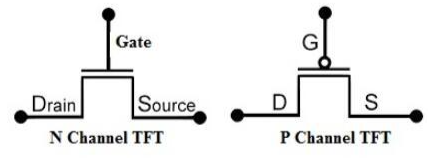
In order to display the information on the screen with high contrast, high brightness, and fast speed, each individual pixel of an LCD (liquid crystal display) contains a thin film transistor, a type of FET or field-effect transistor. The symbol for a thin film transistor is displayed below.

Working Principle of a Thin Film Transistor
These thin film transistors function as individual switches that let the pixels swiftly change positions to turn on and off more quickly. These transistors are the LCDs’ active components and are arranged in a matrix so that the LCDs can display data. These are employed in a variety of commercial display applications, including head-up displays and detectors for digital radiography.
If you want to learn more different types of transistors, you can look at this Electronic Part which is an electronic platform to get more detailed information about transistors such as ULN2003A transistors. ULN2003A is a high-voltage, high-current Darlington transistor array. It has the characteristics of high current gain, high working voltage, wide temperature range, and strong load capacity. It is suitable for all kinds of systems requiring high-speed and high-power driving. Therefore, ULN2003A is used as a high-current driver. Load chip use.
Thin Film Transistor Construction
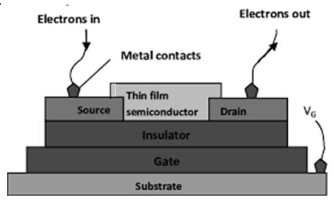
A TFT is a particular kind of Field Effect Transistor that is created by merely depositing thin layers of the active semiconductor layer, dielectric layer, and gate electrode layer on a malleable substance known as substrate. Below is a diagram illustrating the thin film transistor’s construction.

The TFT is made up of various layers made from various materials. So, below is a discussion of the materials used in each layer. The flexible substrate that serves as the first layer of a TFT is constructed from thin metals, glass, and polymers like polyethylene terephthalate. This layer serves as the foundation upon which the electronic device is built.
The gate electrode, which makes up the second layer, can be made of aluminum, gold, or chromium depending on the application. This gate electrode sends a signal to the thin film semiconductor that causes the source and drain to make contact with one another.
The third layer, an insulator, is used to prevent electrical shorting between the gate electrode and the semiconductor layer. The electrode layer, which is the fourth layer, is simply placed on semiconducting surfaces and is made of several conductors, including silver, chromium, aluminum, and gold. Indium Tin Oxide (ITO) is employed even for the source and drain electrodes’ conducting coating. A ceramic or polymer substance encases the entire device.
How Should a Thin Film Transistor Be Connected?
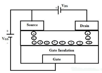
The thin film transistor’s connection diagram is displayed below. In this instance, p-type semiconductor material is used. Polarities will be reversed if n-type material is used. When the transistor is biased by applying a negative voltage between the drain and source contacts, the transistor operates (VDS).

There won’t be any charge between the source and drain contacts when the transistor is off. Therefore, there can be no current flow between the source and drain connections. A negative bias voltage is given to the gate terminal to switch on the transistor (VGS). Therefore, in semiconductors, charge carriers like holes will gather at the gate insulator to form a channel that permits the current (ID) to flow from drain to source.
Difference between a MOSFET and a thin film transistor
| Thin Film Transistor | MOSFET |
| TFTs are typically found in LCDs. | These are utilized in communications, industrial, and automotive systems. |
| TFTs enable the pixels to change conditions quickly, causing them to turn on and off very quickly. TFTs are used as individual switches in LCDs. | MOSFETs are used in circuits to switch or amplify voltages. |
| Different semiconductor materials, including silicon, zinc oxide, and cadmium selenide, are used to create TFTs. | Polycrystalline silicon, high-k dielectric, and silicon carbide are the materials used to create MOSFETs. |
| A type of field-effect transistor where the dielectric substrate is covered with a thin film to create the electrically conducting layer. | A particular type of field-effect transistor has a tiny film of silicon oxide positioned between the gate and the channel. |
| TFT stands for Thin Film Transistor. | MOSFET stands for metal oxide semiconductor field effect transistor. |
Pros and cons of thin film transistors:
The pros of thin film transistors include the following:
- They consume less power.
- They have a quicker reaction time.
- TFTs play a key role in the digital display industry.
- Thin-film transistors are key elements of flexible electronics which are implemented on economical substrates
- They have fast, higher & accurate response rates.
- The TFT-based displays have sharp visibility.
- The physical design of TFT-based displays is excellent.
- It reduces eye strain.
The cons of thin film transistors include the following:
- They depend on backlighting to give brightness instead of generating their own light, so they need in-built LEDs in their backlighting arrangement.
- Restricted utility because of glass paneling.
- The modules of TFTs can only be read once the LEDs are ON.
- TFTs can drain a battery very quickly.
- TFT LCDs are expensive compared to typical monochrome displays.
Applications of thin film transistors
- Smartphones, computers, flat-panel displays, personal digital assistants, and video game consoles all frequently use thin-film transistors.
- TFT LCDs are the best-known application for thin-film transistors, and these transistors are important for today’s materials chemistry and digital displays.
- TFTs are utilized in a variety of foreign applications, including flat panel displays, organic LEDs, and other electronic devices.
- In many X-ray detectors, TFTs are used as sensors.
- Numerous sensing applications use TFT devices.
- TFT LCDs are used in projectors, handheld devices, TVs, personal digital assistants, game consoles, and dashboards in automobiles.